- 您现在的位置:买卖IC网 > Sheet目录338 > LTC3201EMS#TRPBF (Linear Technology)IC LED DRVR WHITE BCKLGT 10-MSOP
LTC3201
TYPICAL APPLICATIO
to place the output capacitor as close to the pin as possible
to minimize inductive ringing and parasitic resistance.
Thermal Management
For higher input voltages and maximum output current
there can be substantial power dissipation in the
LTC3201. If the junction temperature increases above
approximately160 ° C the thermal shutdown circuitry will
automatically deactivate the output. To reduce the maxi-
mum junction temperature, a good thermal connection to
PC board is recommended. Connecting the GND pin (Pin
4) to a ground plane, and maintaining a solid ground plane
under the device on two layers of the PC board can reduce
the thermal resistance of the package and PC board
system.
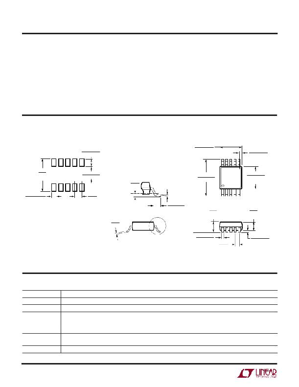
PACKAGE DESCRIPTIO
MS Package
0.889 ± 0.127
(.035 ± .005)
10-Lead Plastic MSOP
(Reference LTC DWG # 05-08-1661)
3.00 ± 0.102
(.118 ± .004)
(NOTE 3)
10 9 8 7 6
0.497 ± 0.076
(.0196 ± .003)
REF
5.23
(.206)
MIN
3.05 ± 0.38
(.0120 ± .0015)
3.2 – 3.45
(.126 – .136)
0.50
(.0197)
GAUGE PLANE
0.254
(.010)
DETAIL “A”
0 ° – 6 ° TYP
4.88 ± 0.10
(.192 ± .004)
1 2 3 4 5
3.00 ± 0.102
(.118 ± .004)
NOTE 4
TYP
BSC
RECOMMENDED SOLDER PAD LAYOUT
WITHOUT EXPOSED PAD OPTION
DETAIL “A”
0.53 ± 0.01
(.021 ± .006)
1.10
(.043)
MAX
0.86
(.034)
REF
0.18
(.007)
SEATING
NOTE:
1. DIMENSIONS IN MILLIMETER/(INCH)
2. DRAWING NOT TO SCALE
3. DIMENSION DOES NOT INCLUDE MOLD FLASH, PROTRUSIONS OR GATE BURRS.
MOLD FLASH, PROTRUSIONS OR GATE BURRS SHALL NOT EXCEED 0.152mm (.006") PER SIDE
4. DIMENSION DOES NOT INCLUDE INTERLEAD FLASH OR PROTRUSIONS.
PLANE
0.17 – 0.27
(.007 – .011)
0.50
(.0197)
TYP
0.13 ± 0.05
(.005 ± .002)
MSOP (MS) 1001
INTERLEAD FLASH OR PROTRUSIONS SHALL NOT EXCEED 0.152mm (.006") PER SIDE
5. LEAD COPLANARITY (BOTTOM OF LEADS AFTER FORMING) SHALL BE 0.102mm (.004") MAX
RELATED PARTS
PART NUMBER
LTC1682/-3.3/-5
LTC1751/-3.3/-5
LTC1754-3.3/-5
LTC1928-5
LT1932
LTC3200/-5
LTC3202
DESCRIPTION
Doubler Charge Pumps with Low Noise LDO
Doubler Charge Pumps
Doubler Charge Pumps with Shutdown
Doubler Charge Pumps with Low Noise LDO
Low Noise Boost Regulator LED Driver
Low Noise Doubler Charge Pump
Low Noise High Efficiency Charge Pump
COMMENTS
MS8 and SO-8 Packages, I OUT = 80mA, Output Noise = 60 μ V RMS
V OUT = 5V at 100mA, V OUT = 3.3V at 80mA, ADJ, MSOP Packages
ThinSOT TM Package, I Q = 13 μ A, I OUT = 50mA
ThinSOT Output Noise = 90 μ V RMS , V OUT = 5V, V IN = 2.7V to 4.4V
ThinSOT Package, High Efficiency, up to 16 LEDs
MS8 and ThinSOT (LTC3200-5) Package, I OUT = 100mA,
2MHz Fixed Frequency
MS10 Package, 125mA Output, High Efficiency
ThinSOT is a trademark of Linear Technology Corporation.
3201f
(408) 432-1900 q FAX: (408) 434-0507 www.linear.com
8
Linear Technology Corporation
1630 McCarthy Blvd., Milpitas, CA 95035-7417
q
LT/TP 0102 2K ? PRINTED IN USA
? LINEAR TECHNOLOGY CORPORATION 2001
发布紧急采购,3分钟左右您将得到回复。
相关PDF资料
LTC3202EDD#PBF
IC LED DRIVR WHITE BCKLGT 10-DFN
LTC3205EUF#TRPBF
IC LED DRVR WT/RGB BCKLGT 24-QFN
LTC3206EUF#TRPBF
IC LED DRVR WT/RGB BCKLGT 24-QFN
LTC3207EUF-1#TRPBF
IC LED DRIVR QVGA DISPLAY 24-QFN
LTC3208EUH#TRPBF
IC LED DRIVR QVGA DISPLAY 32-QFN
LTC3209EUF-2#TRPBF
IC LED DRIVR QVGA DISPLAY 20-QFN
LTC3210EPD-1#TRPBF
IC LED DRVR WHITE BCKLT 16-UTQFN
LTC3210EUD#TRPBF
IC LED DRIVR WHITE BCKLGT 16-QFN
相关代理商/技术参数
LTC3202
制造商:LINER 制造商全称:Linear Technology 功能描述:Low Noise, High Efficiency Charge Pump for White LEDs
LTC3202EDD
功能描述:IC LED DRIVR WHITE BCKLGT 10-DFN RoHS:否 类别:集成电路 (IC) >> PMIC - LED 驱动器 系列:- 产品培训模块:Lead (SnPb) Finish for COTS
Obsolescence Mitigation Program 标准包装:2,500 系列:- 恒定电流:- 恒定电压:- 拓扑:升压(升压),切换式电容器(充电泵) 输出数:1 内部驱动器:是 类型 - 主要:背光 类型 - 次要:白色 LED 频率:625kHz ~ 875kHz 电源电压:2.7 V ~ 5.3 V 输出电压:5V 安装类型:表面贴装 封装/外壳:10-TFSOP,10-MSOP(0.118",3.00mm 宽) 供应商设备封装:10-µMAX 包装:带卷 (TR) 工作温度:-40°C ~ 85°C
LTC3202EDD#PBF
功能描述:IC LED DRIVR WHITE BCKLGT 10-DFN RoHS:是 类别:集成电路 (IC) >> PMIC - LED 驱动器 系列:- 标准包装:60 系列:- 恒定电流:- 恒定电压:- 拓扑:线性(LDO),PWM,升压(升压) 输出数:8 内部驱动器:是 类型 - 主要:背光 类型 - 次要:RGB,白色 LED 频率:500kHz ~ 1.5MHz 电源电压:4.75 V ~ 26 V 输出电压:45V 安装类型:* 封装/外壳:* 供应商设备封装:* 包装:* 工作温度:-40°C ~ 85°C
LTC3202EDD#TR
功能描述:IC LED DRIVR WHITE BCKLGT 10-DFN RoHS:否 类别:集成电路 (IC) >> PMIC - LED 驱动器 系列:- 标准包装:6,000 系列:- 恒定电流:- 恒定电压:- 拓扑:开路漏极,PWM 输出数:4 内部驱动器:是 类型 - 主要:LED 闪烁器 类型 - 次要:- 频率:400kHz 电源电压:2.3 V ~ 5.5 V 输出电压:- 安装类型:表面贴装 封装/外壳:8-VFDFN 裸露焊盘 供应商设备封装:8-HVSON 包装:带卷 (TR) 工作温度:-40°C ~ 85°C 其它名称:935286881118PCA9553TK/02-TPCA9553TK/02-T-ND
LTC3202EDD#TRPBF
功能描述:IC LED DRIVR WHITE BCKLGT 10-DFN RoHS:是 类别:集成电路 (IC) >> PMIC - LED 驱动器 系列:- 标准包装:6,000 系列:- 恒定电流:- 恒定电压:- 拓扑:开路漏极,PWM 输出数:4 内部驱动器:是 类型 - 主要:LED 闪烁器 类型 - 次要:- 频率:400kHz 电源电压:2.3 V ~ 5.5 V 输出电压:- 安装类型:表面贴装 封装/外壳:8-VFDFN 裸露焊盘 供应商设备封装:8-HVSON 包装:带卷 (TR) 工作温度:-40°C ~ 85°C 其它名称:935286881118PCA9553TK/02-TPCA9553TK/02-T-ND
LTC3202EMS
功能描述:IC LED DRVR WHITE BCKLGT 10-MSOP RoHS:否 类别:集成电路 (IC) >> PMIC - LED 驱动器 系列:- 标准包装:6,000 系列:- 恒定电流:- 恒定电压:- 拓扑:开路漏极,PWM 输出数:4 内部驱动器:是 类型 - 主要:LED 闪烁器 类型 - 次要:- 频率:400kHz 电源电压:2.3 V ~ 5.5 V 输出电压:- 安装类型:表面贴装 封装/外壳:8-VFDFN 裸露焊盘 供应商设备封装:8-HVSON 包装:带卷 (TR) 工作温度:-40°C ~ 85°C 其它名称:935286881118PCA9553TK/02-TPCA9553TK/02-T-ND
LTC3202EMS#PBF
功能描述:IC LED DRVR WHITE BCKLGT 10-MSOP RoHS:是 类别:集成电路 (IC) >> PMIC - LED 驱动器 系列:- 标准包装:6,000 系列:- 恒定电流:- 恒定电压:- 拓扑:开路漏极,PWM 输出数:4 内部驱动器:是 类型 - 主要:LED 闪烁器 类型 - 次要:- 频率:400kHz 电源电压:2.3 V ~ 5.5 V 输出电压:- 安装类型:表面贴装 封装/外壳:8-VFDFN 裸露焊盘 供应商设备封装:8-HVSON 包装:带卷 (TR) 工作温度:-40°C ~ 85°C 其它名称:935286881118PCA9553TK/02-TPCA9553TK/02-T-ND
LTC3202EMS#TR
功能描述:IC LED DRVR WHITE BCKLGT 10-MSOP RoHS:否 类别:集成电路 (IC) >> PMIC - LED 驱动器 系列:- 标准包装:6,000 系列:- 恒定电流:- 恒定电压:- 拓扑:开路漏极,PWM 输出数:4 内部驱动器:是 类型 - 主要:LED 闪烁器 类型 - 次要:- 频率:400kHz 电源电压:2.3 V ~ 5.5 V 输出电压:- 安装类型:表面贴装 封装/外壳:8-VFDFN 裸露焊盘 供应商设备封装:8-HVSON 包装:带卷 (TR) 工作温度:-40°C ~ 85°C 其它名称:935286881118PCA9553TK/02-TPCA9553TK/02-T-ND
